Enabling PCB Layout and Reading the Board for the First Time
Requirement: the project already has components + wires saved in the Diagram tab (if not, the PCB Editor will show "You need to add and save components in the Diagram before viewing the PCB").
Steps
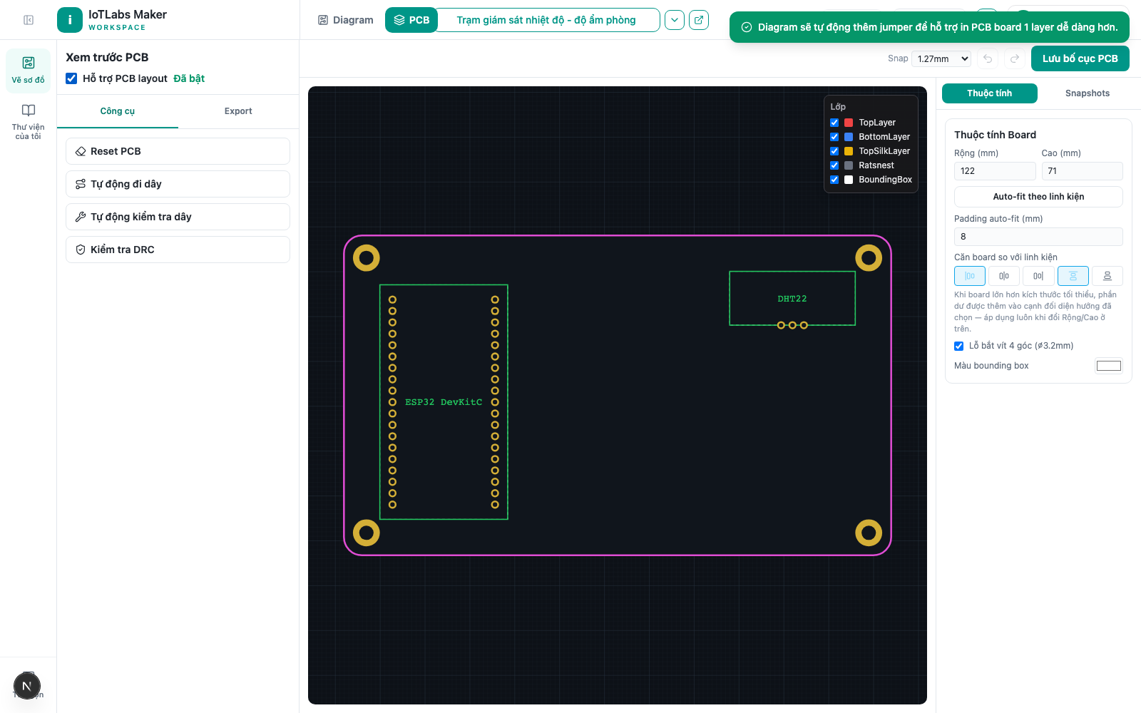
- Go to the PCB tab. If you've never enabled it before, you'll see the message "Enable 'PCB Layout Support' to design the PCB layout..." and a status label showing Disabled.
- Check the PCB Layout Support checkbox at the top of the page.
- The system saves the state and shows a confirmation toast; the label changes to Enabled.
Result: The board appears with a board outline, a silkscreen layer (component outlines), pads/drill holes, mounting holes in all 4 corners, and, most importantly, the ratsnest layer — thin straight lines (virtual lines, not yet real copper traces) connecting pairs of pads according to each net already present in the Diagram. Each net that hasn't been routed = 1 ratsnest line.
Note
The PCB has only 1 copper layer (single-layer, suited to making it yourself at home) — this is why 2 traces crossing on the board is a real error here, unlike a multi-layer industrial PCB.
Example
After enabling PCB layout for the "Room Temperature & Humidity Monitoring Station," the board shows 3 thin ratsnest lines connecting the ESP32 and DHT22 (matching the 3 VCC/GND/DATA wires already connected in the Diagram) — no real copper traces yet, this is the preparation step before routing.