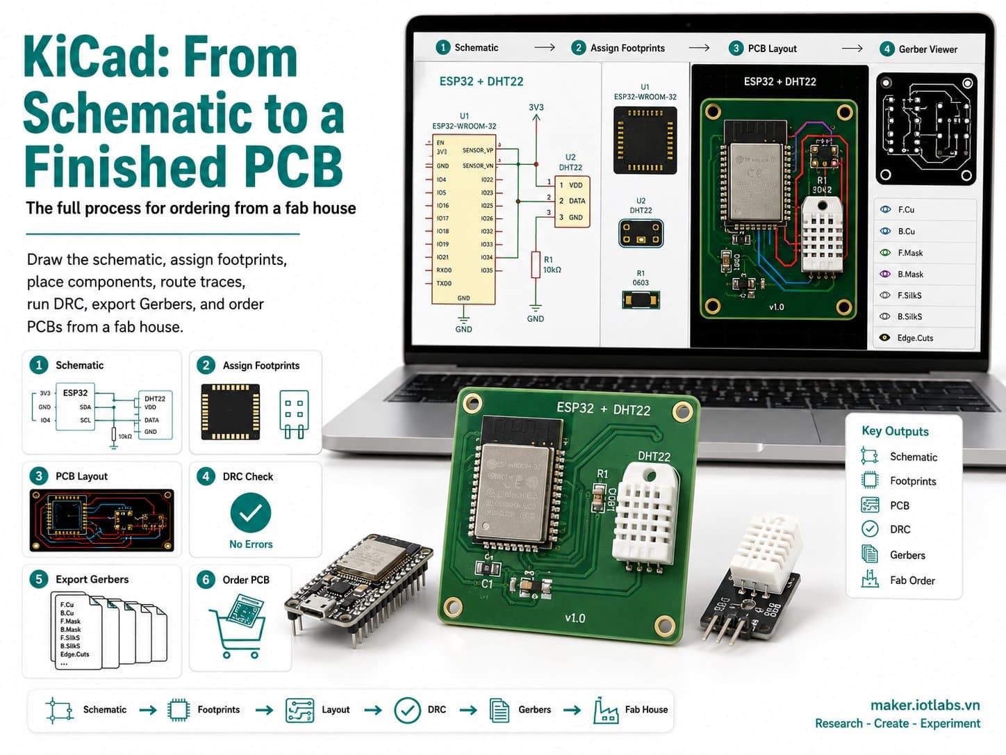
KiCad: From Schematic to a Finished PCB — the Full Process for Ordering from a Fab House
Going from an ESP32 + DHT22 breadboard prototype to a finished PCB: drawing the schematic in Eeschema, assigning footprints, laying it out in the PCB Editor, running DRC, and exporting Gerbers to order from a fab house.
This guide walks through the entire PCB design process in KiCad, from schematic to order-ready Gerber files, using an ESP32 DevKit V4 + DHT22 sensor circuit as a real running example throughout.
Detailed guide
The complete schematic-to-PCB workflow in KiCad: drawing the schematic, assigning footprints, PCB layout, DRC, and exporting Gerbers, illustrated with a real ESP32 + DHT22 circuit.
1. Introduction
Once a breadboard prototype is running reliably, the next step toward turning it into a real product is PCB (Printed Circuit Board) design. KiCad is a free, open-source EDA (Electronic Design Automation) tool widely used both in the maker community and in industry. This guide covers the full standard "schematic to PCB" workflow in KiCad — drawing the schematic (Eeschema), assigning real component footprints, arranging and routing on the PCB Editor, running design rule checks (DRC), and finally exporting Gerber files to order from a fab house.
To keep this from being pure theory, the guide uses one real circuit as the running example throughout: an ESP32 DevKit V4 reading a DHT22 temperature/humidity sensor over a single digital GPIO. This circuit has already been built on a breadboard, flashed, and run for real (full code in section 5) — it's exactly this circuit that we'll turn into a schematic and PCB in the steps that follow.
2. Components Needed
Component | Qty | Notes |
|---|---|---|
ESP32 DevKit V4 | 1 | The main control board — dual-core 240MHz, WiFi/BLE |
DHT22 (AM2302) | 1 | A temperature/humidity sensor using a 1-Wire-style interface |
10kΩ resistor | 1 | Pull-up for the DHT22's DATA pin — recommended by the datasheet |
Breadboard + jumper wires | 1 set | For building the prototype circuit before moving to PCB |
3. Wiring Diagram (the prototype circuit)
DHT22 | ESP32 DevKit V4 |
|---|---|
VCC | 3V3 |
GND | GND |
DATA | GPIO4 (via a 10kΩ pull-up resistor to 3V3) |
This is exactly the circuit we'll turn into a KiCad schematic in the next section. The three signals (VCC, GND, DATA) correspond to three nets in the schematic.
4. The Complete Workflow: From Schematic to Gerber in KiCad
Step 1 — Draw the Schematic in Eeschema
Create a new KiCad project and open the Schematic Editor (Eeschema). Place a symbol for each part in the real circuit above: an MCU/module symbol for the ESP32 DevKit (or a header symbol if you're plugging in a separate board onto a carrier PCB), a symbol for the DHT22 (3 pins: VCC, GND, DATA/OUT), and a 10kΩ resistor symbol. Wire them up exactly as shown in the wiring table in section 3: DHT22 VCC to 3V3, GND to GND, and DATA to an ESP32 GPIO pin (e.g. GPIO4) while also connecting through the 10kΩ resistor to the 3V3 rail (pull-up).
Once it's drawn, use Annotate Schematic Symbols to have KiCad automatically number each part's reference designator (U1, R1, J1...), avoiding duplicates. Run Electrical Rules Check (ERC) to catch issues early — unconnected pins, output-output conflicts, or missing power.
Step 2 — Assign Footprints to Each Component
A footprint is a component's physical "footprint" on the PCB — pad size, pin spacing, mounting type (through-hole or SMD). Use the Assign Footprints tool (the Footprint Assignment Tool) to match each schematic symbol to a real library footprint: the DHT22 uses a 3-pin THT header footprint at 2.54mm pitch (matching the real module), the 10kΩ resistor uses either a THT axial or an 0805 SMD footprint depending on which type you actually have, and the ESP32 DevKit is typically mounted as a module directly on the board, or via a header footprint plugged into the main board. This step is mandatory — without footprints, the netlist can't be transferred to the PCB Editor.
Step 3 — Move to the PCB Editor and Route
From Eeschema, use Update PCB from Schematic to bring the whole netlist and its footprints into the PCB Editor. The components appear as a cluster of parts connected by "ratsnest" lines (straight-line previews) showing which logical connections still need routing. Next:
Draw the board outline (Edge.Cuts layer) at the size and shape you want.
Place components sensibly — the DHT22 should sit near the board edge, away from heat sources, since it measures ambient temperature.
Route each ratsnest connection: the signal trace (DATA) can use the standard minimum width (0.25mm), while power traces (3V3, GND) should be wider to handle more current — you can calculate this with a track-width calculator based on the ESP32's actual current draw.
Optionally, pour a copper zone for GND to create a ground plane, reducing noise and impedance.
Step 4 — Design Rule Check (DRC)
Before exporting production files, always run DRC in the PCB Editor. DRC checks minimum spacing between traces/pads (clearance), whether any net is left unrouted, whether drill hole sizes are valid for the chosen copper thickness, and other design-rule violations set under Board Setup → Design Rules. A PCB isn't considered done while DRC still reports errors.
Step 5 — Export Gerbers and Double-Check
Use File → Fabrication Outputs → Gerbers to export the needed layers: top/bottom copper (F.Cu/B.Cu), soldermask (F.Mask/B.Mask), silkscreen (F.Silkscreen/B.Silkscreen), board outline (Edge.Cuts), along with the drill file (Excellon format). After exporting, reopen the full set in a Gerber viewer (built into KiCad) for a visual check: do the layers line up correctly, is anything missing, is there any unusual geometry — this is the final cross-check before sending it to a fab.
Step 6 — Order from a PCB Fab
The ordering process is broadly similar across most PCB fabs: zip up all the Gerber and drill files, upload them to the fab's ordering system, which parses them automatically and shows a preview for you to confirm layer count, board dimensions, thickness, and soldermask color before paying. Reference pricing for a small run of a 2-layer prototype PCB is usually a few dollars a board, depending on the fab and turnaround time — but the actual cost depends heavily on layer count, dimensions, quantity, and vendor, so treat this as a general process, not a specific quote.
5. ESP32 + DHT22 Sample Code (the real circuit used as the example)
#include <DHT.h>

#define DHTPIN 4
#define DHTTYPE DHT22

DHT dht(DHTPIN, DHTTYPE);

const unsigned long TELEMETRY_INTERVAL_MS = 2000;
unsigned long lastTelemetryAt = 0;

void setup() {
  Serial.begin(115200);
  delay(200);
  Serial.println();
  Serial.println(F("=== ESP32 + DHT22 - Vi du minh hoa cho bai viet KiCad/PCB ==="));
  Serial.println(F("Boot OK. Khoi tao cam bien DHT22..."));

  dht.begin();

  Serial.println(F("San sang doc du lieu."));
}

void loop() {
  unsigned long now = millis();
  if (now - lastTelemetryAt >= TELEMETRY_INTERVAL_MS) {
    lastTelemetryAt = now;

    float humidity = dht.readHumidity();
    float temperatureC = dht.readTemperature();

    Serial.print(F("{\"temperature_c\":"));
    if (isnan(temperatureC)) {
      Serial.print(F("null"));
    } else {
      Serial.print(temperatureC, 1);
    }
    Serial.print(F(",\"humidity_pct\":"));
    if (isnan(humidity)) {
      Serial.print(F("null"));
    } else {
      Serial.print(humidity, 1);
    }
    Serial.print(F(",\"uptime_ms\":"));
    Serial.print(now);
    Serial.println(F("}"));

    if (isnan(humidity) || isnan(temperatureC)) {
      Serial.println(F("[WARN] Doc cam bien DHT22 that bai - kiem tra day noi hoac dien tro keo len DATA."));
    }
  }
}
6. Mapping the Real Circuit to the Schematic
Real circuit (breadboard) | In the KiCad schematic |
|---|---|
Red wire: DHT22 VCC → ESP32 3V3 | The "3V3" net connects the DHT22 symbol's VCC pin and the ESP32 symbol's 3V3 pin |
Black wire: DHT22 GND → ESP32 GND | The "GND" net (usually assigned a global GND label) |
Yellow wire: DHT22 DATA → GPIO4 | The signal net connecting DATA and GPIO4, with a branch through R1 (10kΩ) to 3V3 |
The standalone resistor plugged into the breadboard | A Device:R symbol with a value of 10k, later assigned a matching THT/SMD footprint |
Mapping it out this way helps beginners see clearly: a schematic isn't some abstract concept — it's an electrical drawing with the exact same connection structure as the breadboard circuit that's already running. The only difference is that it's standardized so a computer can understand it and automatically generate manufacturing files.
7. Common Issues
Issue | Cause | Fix |
|---|---|---|
PCB Editor reports "Footprint not found" | The schematic symbol hasn't been assigned a footprint | Re-run Assign Footprints, and check that the footprint library has been added to the project |
DRC reports "Clearance violation" | Two traces/pads are placed closer together than the design rules allow | Increase the trace spacing, or adjust Board Setup → Design Rules to match your fab's capabilities |
Exported Gerbers are missing the Edge.Cuts layer | Forgot to enable the board outline layer when exporting Fabrication Outputs | Double-check the selected layer list in the Plot dialog before exporting |
DHT22 readings always return NaN after moving to PCB | Missing pull-up resistor on the DATA trace, or the trace is too long without a pull-up to stabilize the signal | Make sure R1 (10kΩ) is placed close to the DATA pin and correctly connected to 3V3 on the actual layout, not just in the schematic |
8. Summary
The "schematic to PCB" workflow in KiCad boils down to six core steps: draw and annotate the schematic, assign footprints, move to the PCB Editor and route, run DRC, export Gerbers, and order from a fab.
Each step has its own verification tool (ERC for the schematic, DRC for the PCB, a Gerber viewer for the exported files) — using all of them thoroughly minimizes the risk of having to redo a board because of a design mistake.
The ESP32 + DHT22 circuit in this guide has only 3 signals, but it's enough to illustrate the entire workflow; for more complex circuits (more sensors, more copper layers), the same steps still apply — the only difference is the complexity of routing and the number of DRC rules to satisfy.